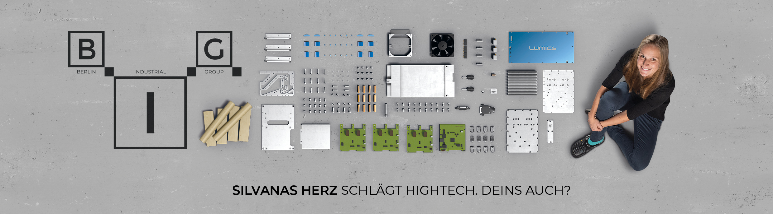
Lumics GmbH - as a member of B.I.G. Berlin Industrial Group - is a key player for design and manufacturing of diode lasers for demanding medical, industrial and scientific applications. In-house capabilities range from chip level up to fiber-coupled diode laser modules and full solutions including OEM drivers and cooling plates.
We are looking for a Senior Laser Diode Packaging Engineer with specialized expertise in microoptics, submounts, optics, and sealing technologies to join our team. In this pivotal role, you will take ownership of the product lifecycle for high-performance laser diodes, from packaging design and development through to production, ensuring the product meets all technical, reliability, and performance standards. You will collaborate closely with optical, mechanical, and electrical engineers to create robust, reliable, and cost-effective packaging solutions for laser diodes in diverse applications, including telecommunications, medical devices, and industrial systems.
- Product Ownership: Take full responsibility for laser diode packaging products, from concept through to transfer to production
- Packaging Design: Lead the design and development of advanced packaging solutions for high-performance laser diodes, with a focus on integrating microoptics, submounts, and optical components to optimize functionality.
- Optical Integration: Design and implement optical alignment and coupling methods, ensuring high-efficiency light extraction and minimal optical loss.
- Submount and Thermal Management: Design and develop submounts for laser diodes that ensure effective heat dissipation and optimal thermal management, using materials and methods that guarantee long-term reliability.
- Sealing Technologies: Develop and implement advanced sealing technologies (such as hermetic and adhesive bonding) to ensure environmental protection and prevent degradation over time.
- Reliability and Testing: Oversee the testing and validation of packaging solutions, performing rigorous reliability testing and failure analysis (e.g., accelerated life tests, thermal cycling, and optical performance evaluation).
- Cross-functional Collaboration: Work closely with cross-disciplinary teams (mechanical engineering, electrical engineering, and manufacturing) to integrate packaging solutions with the overall system design.
- Process Improvement: Identify and drive improvements in packaging technologies, materials, and processes to reduce cost, improve performance, and increase yield.
- Vendor Management: Support the purchasing department with suppliers to source packaging materials, components, and tools, ensuring high-quality standards and adherence to project timelines.
- Documentation and Reporting: Prepare comprehensive technical documentation, including design specifications, test results, and reliability reports. Present design progress, test results, and solutions to internal and external stakeholders.
- Mentorship: Provide technical leadership and mentorship to junior engineers and technicians, fostering a culture of continuous learning and innovation within the packaging team.
- Project Management: Manage multiple packaging projects simultaneously, ensuring on-time delivery and maintaining high levels of product quality throughout the process.
- Bachelor's or Master's degree in Electrical Engineering, Optics, Materials Science, Physics, or a related field.
- Minimum of 5-7 years of experience in laser diode packaging, optoelectronics, or semiconductor packaging, with a strong focus on microoptics, submounts, and sealing technologies.
- Proven experience in designing and implementing laser diode packaging solutions involving optical integration, submounts, and thermal management.
- Expertise in the application of sealing technologies (hermetic sealing, adhesive bonding, etc.) for optoelectronic components.
- Strong understanding of optical alignment, coupling, and light extraction methods for high-performance laser diodes.
- In-depth knowledge of materials used in laser diode packaging, including metals, ceramics, and polymers.
- Experience with reliability testing of optoelectronic devices and failure analysis techniques.
- Strong project management skills with the ability to lead and coordinate teams across multiple functions.
- Exceptional communication skills, with the ability to present complex technical information to both technical and non-technical stakeholders.
- Ability to work in a fast-paced environment and manage competing priorities.
- Ph.D. in a relevant field (e.g., Optics, Materials Science).
- Experience with high-volume manufacturing processes and scaling packaging solutions for mass production.
- Hands-on experience with simulation tools (e.g., COMSOL, Ansys) for optical, thermal, and mechanical analysis.
- Familiarity with ISO/IEC standards and best practices in packaging and optoelectronics.
- Previous experience in product ownership or as a technical lead for optoelectronic or photonic devices.
- Competitive salary and comprehensive benefits package.
- Opportunity to work on cutting-edge laser diode technologies with a focus on microoptics and advanced packaging solutions.
- Be part of a dynamic team where your technical contributions will drive product innovation and performance.
- Career growth opportunities in a fast-paced and evolving industry.
- Collaborative, innovative work environment with exposure to cross-disciplinary engineering challenges.
|
 - Logo")